Deliver Higher 3D-AOI Detection Accuracy and Efficiency with Basler boost V

What is it all about?
The rapid development of the electronics industry has caused semiconductor components to become essential across most industries. With the volume of electronic components required, manufacturers are becoming increasingly reliant on automated assembly for semiconductors and similar components.
This brings unique quality assurance challenges: manufacturers must inspect extremely large numbers of surface mount components—which continue become smaller—for dimensional accuracy while ensuring high precision.
What was the problem?
Presently, 12-megapixel cameras are the preferred product for 3D AOI solution setups. However, since inspection requirements will continue to become more sophisticated as the rapid development of electronics continues, we are certain this resolution will soon become insufficient.
One option is to reduce the field of view while the camera resolution remains unchanged. Unfortunately, this increases the number of image acquisitions and reduces the detection efficiency—which is not advisable.
The solution
Choosing a suitable system resolution is a key parameter to consider when selecting your 3D-AOI system.
Improved detection accuracy
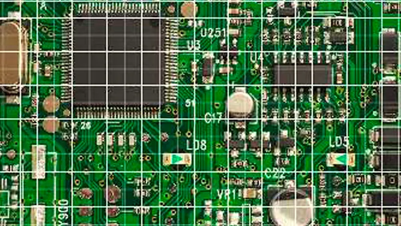
By replacing the existing mainstream 12-megapixel (4096×3070) camera with a 25-megapixel (5120×5120) camera, the rate is increased by more than 1.5x, and the detection accuracy is also improved accordingly.
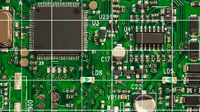
Improved detection efficiency
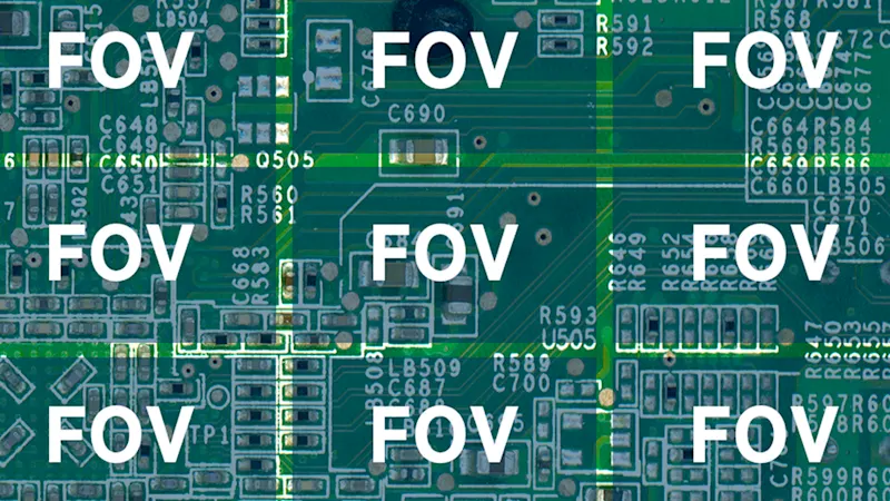
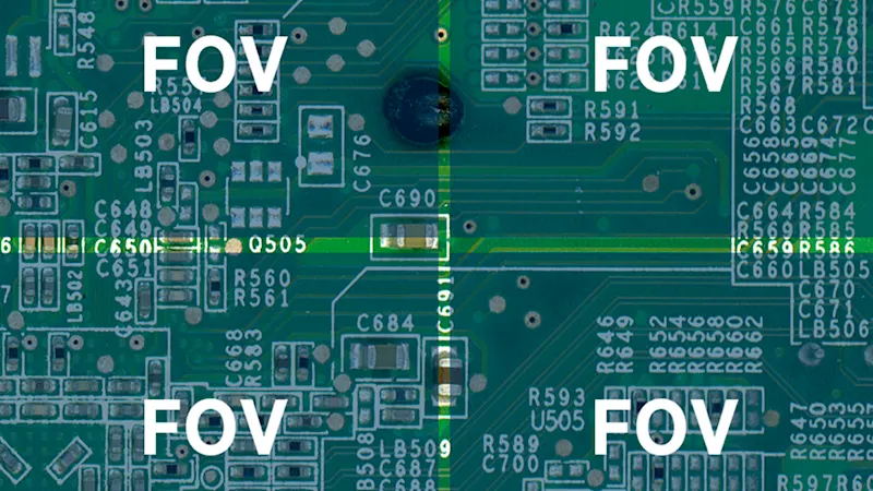
The boost V 25-megapixel camera features a 4-port CXP-12 interface, a total bandwidth of 50 Gbps, and a frame rate up to 150 fps—increasing the image acquisition speed by 1.2x. Meanwhile, if the detection accuracy remains constant or is improved slightly, the area of a single FOV is enlarged. This reduces the number of acquisitions, thus reducing the acquisition time.
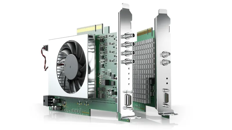
Relocating the image pre-processing algorithm to the matching image acquisition card’s FPGA can effectively reduce the image processing time. Using edge extraction and median filtering as an example, the processing time of the FPGA is less than 50% of the CPU or GPU. Meanwhile, the CPU load is significantly reduced and the overall system stability is improved.
Your benefits
Achieve increased accuracy and productivity at a lower cost
Take full advantage of the FPGA image preprocessing speed to improve processing efficiency, reduce CPU load, and improve overall system stability
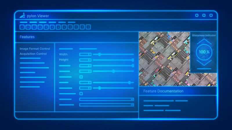
Common SDK for cameras and image acquisition cards makes secondary development easier and more efficient
Receive one-stop product solutions, including: cameras, lenses, light sources, image acquisition cards, cables, and software—all with guaranteed compatibility, efficient operation, low maintenance, and low cost
Receive all-round selection testing and after-sales technical support services
Products for this solution
Looking to implement a comparable solution? These products will help you.
