1µm-Precision Wafer Bonding Inspection Through Alignment Marks with SWIR Cameras
As semiconductor devices shrink and packaging complexity grows, achieving sub-micron alignment in wafer and die bonding is increasingly challenging. Traditional optical inspection struggles with buried alignment marks and subsurface defects, impacting yield and performance. SWIR imaging provides a non-destructive solution, enabling clear visualization through silicon and other materials for precise alignment and defect detection.
Precision alignment: a growing challenge in advanced packaging
As semiconductor packaging advances with technologies like TSV, hybrid bonding, and CoWoS, precise wafer and die bonding becomes critical. Stacking multiple wafers, dies, or chips—such as HBM—demands alignment accuracy down to 1µm. Any misalignment at this scale can compromise interconnect integrity, degrade performance, and reduce yield.

Ensuring precise alignment and defect detection in wafer and die bonding processes presents several challenges that can impact yield and device performance. These include:
Hidden Alignment Marks: Alignment marks often get buried beneath silicon, oxide, or bonding adhesives, making them invisible to traditional optical systems.
High-Contrast Imaging: Alignment marks and small defects can be faint, necessitating high sensitivity and contrast for accurate detection.
SWIR imaging for non-destructive alignment and defect detection
SWIR (Short-Wave Infrared) imaging can penetrate silicon and other materials, revealing hidden alignment marks and bonding interfaces without damaging wafers. However, integrating SWIR into high-precision semiconductor inspection requires addressing critical factors:
Selecting the right sensor to balance sensitivity, cost, and integration complexity
Managing pixel defects inherent to InGaAs sensors
Determining when active cooling (TEC) is necessary and when TEC-less solutions suffice
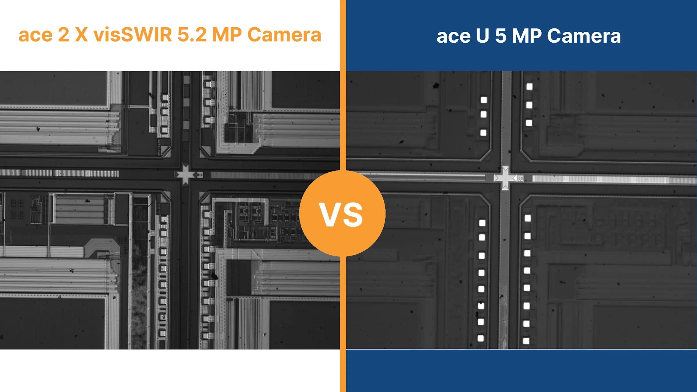
Basler’s SWIR 5.2MP cameras: optimized for semiconductor inspection
Basler’s ace 2 X visSWIR cameras bridge the gap between high-performance cooled SWIR cameras for labs and low-cost solutions for commercial and public safety applications. For high-end industrial use, the camera design must balance cost-efficiency, deliver the required level of precision, and integrate seamlessly into final inspection AOI machines.

Featuring Sony’s SenSWIR sensor, these cameras offer:
High-contrast imaging to detect faint alignment marks and subsurface defects
Real-time pixel defect correction, ensuring clear, distortion-free images
Flexible cooling options tailored to application needs without unnecessary complexity
Next steps: test your samples with our vision experts
Send in your samples, and our team will evaluate the best SWIR components for your application, ensuring the ideal balance of performance, cost, and integration efficiency.
Request a free sample testBeyond alignment: SWIR applications in semiconductor inspection

Beyond wafer bonding and die alignment, SWIR imaging enhances various semiconductor inspection processes, offering deeper material penetration and high-contrast defect detection. SWIR cameras are widely used for ingot and wafer inspection, defect detection, wire bonding analysis, and yield optimization. Their ability to penetrate silicon and other materials enables comprehensive quality control across multiple stages of semiconductor manufacturing.
SWIR imaging: essential for next-gen 2.5D & 3D packaging
With its ability to see through silicon and other semiconductor materials, SWIR imaging is transforming semiconductor inspection across multiple applications. From precise alignment in advanced packaging to defect detection and yield optimization, its impact is undeniable.
SWIR imaging is now a practical solution for semiconductor OEMs, enabling precise alignment and defect detection for next-generation 2.5D and 3D packaging. Basler offers not just SWIR cameras but a deep understanding of semiconductor inspection challenges—delivering engineered solutions with guaranteed precision, without overcomplication.
Contact usProducts for this solution
Looking to implement a comparable solution? These products will help you.


