Optimizing Wafer and Die Inspections: High-Speed, High-Precision Vision Architecture
As the semiconductor industry advances toward higher performance and smaller sizes, defect inspection of wafers and dies becomes increasingly critical in advanced packaging processes. Especially in high-tech applications such as 5G, artificial intelligence (AI), and the Internet of Things (IoT), the demand for semiconductor component quality continues to rise—placing higher requirements on precision inspection technologies.
Wafer and die inspection targets
In semiconductor manufacturing, wafer surface inspection and die inspection are two important but distinct stages of quality control:
Wafer surface inspection targets the entire wafer, focusing on macroscopic defects such as contamination, scratches, pattern misalignment, and structural integrity during the manufacturing processes. Vision inspection systems require a large field of view and high-speed scanning capabilities to cover the entire wafer surface.
Die inspection focuses on detailed analysis of individual dies, emphasizing microscopic defects such as edge chipping, poor dicing, and internal structural issues.
Four major challenges in wafer and die AOI inspection
CPU bottlenecks in high-speed, real-time image processing Wafer and die inspections require processing massive volumes of high-resolution images—often 25 MP or more, with hundreds of thousands of images per unit. These inspections must be completed in fractions of a second, especially for die inspection (within 0.7 seconds). Traditional CPU-based systems often struggle under this load, leading to delays, limited throughput, and inefficient data handling that slow down both development and production.
Lack of flexible algorithms and low adaptability Fixed algorithms struggle to detect irregular or low-contrast defects and have difficulty handling special materials like silicon carbide (SiC) and gallium nitride (GaN), which have unique reflective properties. When die size, materials, or structures change, existing algorithms may not adapt quickly, reducing detection accuracy and extending development time.
Difficulty in detecting microscopic defects In advanced packaging processes, detecting tiny surface defects—such as micro-cracks or contamination—becomes increasingly challenging, especially as defect sizes approach the resolution limits of the camera and optics.
Complexity of high-reflectivity surface inspection Reflective surfaces, like wafer and die surfaces, and metal layers, are hard to inspect with standard optics, often causing false positives or missed defects.
Edge processing: building a more efficient vision inspection architecture
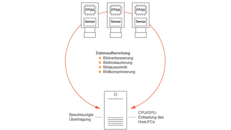
To address these challenges, we propose a vision system architecture that shifts processing to the edge—at the camera and frame grabber—where raw data is filtered, and only valuable information is retained.
Customized cameras with built-in algorithms to reduce CPU load
Common preprocessing tasks—such as lens distortion correction, HDR, flat-field correction (FFC), autofocus, and background subtraction—are embedded directly into the FPGA within the camera. This allows image processing to occur before reaching the CPU, greatly reducing backend load and improving real-time performance.
Programmable frame grabbers for algorithm flexibility
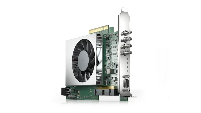
For more complex or resource-intensive algorithms, programmable frame grabbers offer a flexible platform to deploy image pre-processings such as image stitching or focus stacking. Using graphical programming software like VisualApplets significantly accelerates development and validation cycles.
High-quality optical systems: the key to inspection accuracy
Accurate identification of tiny scratches, cracks, and contaminants on highly reflective wafer and die surfaces relies on the optical setup and sensor choice—both of which play a decisive role in image quality.
Advanced illumination and optical design
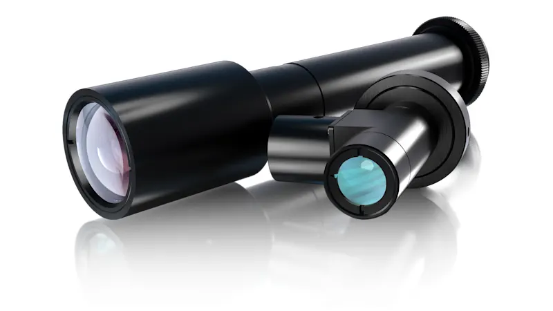
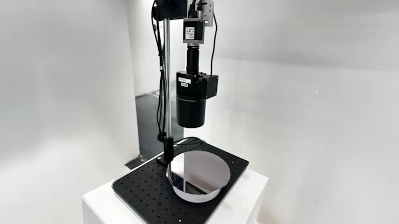
Adjustable-aperture telecentric lenses and coaxial lighting enable parallel light design, minimizing stray light interference and significantly improving inspection accuracy. Such systems provide optimal lighting for materials with varying reflectivity, ensuring critical defect features are captured effectively.
Consult an optical expertHigh quantum efficiency imaging
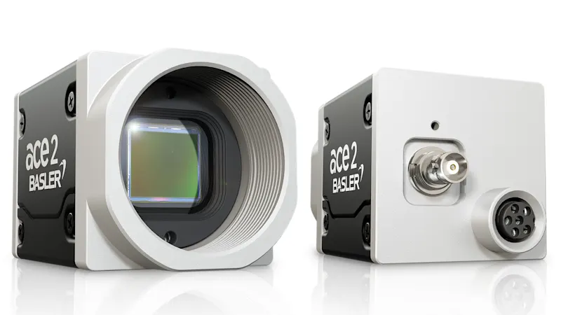
For 25 MP resolution cameras, Basler’s ace 2 V 25 MP camera stands out with industry-leading quantum efficiency. It captures more photons under high-speed, low-light conditions, resulting in higher-contrast images. This makes it easier to detect subtle wafer or die defects even under poor lighting or low contrast. The combination of high quantum efficiency sensors and professional lighting systems forms a solid hardware foundation for microscopic defect detection.
Request to testEmpowering next-generation semiconductor inspection
To unlock the full potential of high-performance image sensor technology, it’s essential to partner with quality camera manufacturers. Choosing and testing the right high-performance optical system—without overengineering—is just as important. Last but not least, effectively integrating front-end image acquisition system with a powerful backend vision processing architecture lays a solid foundation for next-generation semiconductor inspection.
Optimizing AI inference performance
AI models are widely adopted to enhance defect detection accuracy and speed. The next challenge is boosting inference performance—ensuring faster and more stable results while avoiding wasted computational effort on irrelevant data. By filtering data at the front-end using smart cameras and frame grabbers, only relevant image regions or defect features are passed downstream to the CPU or GPU, enhancing AI model efficiency. High-quality images captured by high quantum efficiency cameras also provide more reliable input for AI, significantly reducing false positives.
Modular and scalable system design
This architectural approach meets next-generation visual inspection needs in advanced packaging with higher demands for flexibility and scalability. OEMs can quickly adapt algorithm modules in response to process changes—deploying different image processing logic across various stages (front-end wafer, mid-stage die attach, back-end packaging) without altering the core system. Integrating high-performance optical systems with intelligent preprocessing not only addresses current challenges but also paves the way for future system upgrades.
Get in touch with a vision engineerSummary: perfect balance of accuracy and speed
In today’s increasingly competitive semiconductor manufacturing landscape, improving yield while reducing time-to-market is a critical competitive edge. Our solution combines edge processing, optimized optical systems, and high-quality imaging to overcome fundamental AOI inspection challenges for wafers and dies.
By shifting image preprocessing to the camera and frame grabber and pairing it with high quantum efficiency imaging and specialized lighting, we achieve the perfect balance of precision and speed. This integrated approach not only enhances defect detection for microscopic flaws but also boosts overall system performance—offering semiconductor manufacturers a reliable, efficient, and future-ready AOI inspection foundation.
Products for this solution
Looking to implement a comparable solution? These products will help you.
